SemiSoft Knowledge
Learn more about our experiences and the knowledge we gained working more than 25 years in the semiconductor industry. In this section you will find a variety of insights from SHK Engineering and Consulting (www.shk.com), the company behind SemiSoft®.
Good Design pays for itself
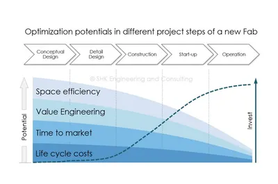
The potential to achieve high space efficiency is particularly high at the start of the design process. When investments get higher, good Fab design pays very much for itself.
Is there a perfect Fab design?
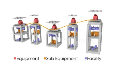
All modern 300mm front-end fabs have similar functional areas, yet almost no two fab buildings share the same dimensions. Modern 3D design is one key to more compact results.
The level of detail should fit the task
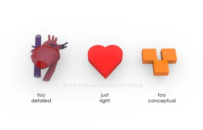
A solid that looks like a pipe but has no references to material and technical data should not be called BIM. At SHK, every 3D component is a real digital twin with embedded data.
Different values of cleanrooms
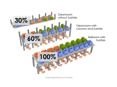
Not only the cleanroom area matters — the type of cleanroom results in relevant space efficiency differences of up to 70%. A closer look at a dry-etch space example.

How big is Giga?
Two fab site plots in the same scale: 17 times bigger site, 14 times bigger cleanroom, 1.2 vs. 24 billion US$ investment. The Gigarace in semiconductor manufacturing is in full swing.
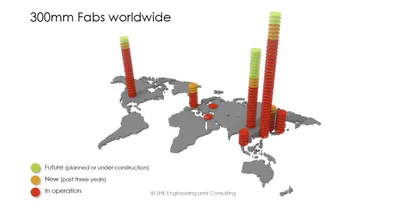
So-called “wafers”
In Europe, the semiconductor industry is still not widely known in all areas needed to build a new fab. Recent projects in Dresden, Villach and Agrate have done a lot for training experts.

Three topics, one solution
Gas detection limits, space management issues from large exhaust pipes, and costly make-up air: SHK has developed a patented exhaust unit that solves all three topics at once.
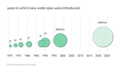
450mm ready
Fab buildings are valuable properties with lifespans measured in decades. Even if it still sounds like the future, modern fab buildings should be 450mm ready.