So-called “wafers”
Semiconductors are manufactured in so-called “Fabs” in an so-called “cleanroom” on so-called “wafers”.
When I started in the semiconductor industry in the 90s, I had to take a test-wafer-carrier with me on my first trip to Japan. The security at Munich Airport looked at the carrier with great interest and knew nothing about the term “wafer”. After a detailed explanation I could luckily pass. Upon arrival in Tokyo, the security noticed the carrier and very obviously knew immediately what it was.
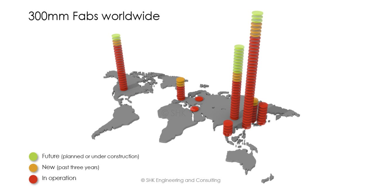
In Europe, the semiconductor industry is still not a widely known industry in all the areas needed to build a new fab. As long as publications contain sentences with “so-called ‘wafers’”, a new fab project will again be a costly search for experienced resources and remain unavoidable a basic training for a part of the engineering- building- and construction team.
Together, however, the recent projects from Bosch in Dresden, Infineon in Villach and STMicroelectronics in Agrate have done a lot for the training of experts in Europe. The momentum could be used even if it will need further strong efforts to build competitive 300mm Fabs or eventually a first Gigafab in Europe and come closer to the design and construction level of what is today state-of-the-art in the Asian semiconductor manufacturing countries.
Comment on LinkedIn